Design of a preamplifier for 144 MHz with 1 dB NF and 23 dB gain using BF981.
Background
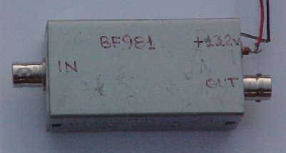
This amplifier is using a low cost silicon MOSFET (BF981 from Philips) to give more than 20 dB gain with around 1 dB noise figure on 2 meter.You can build more advanced low noise amplifiers using GaAs FET's, but the dual gate MOSFET is no bad performer - the difference in noise figure may not even show up on terrestrial path. Besides it's a lot more forgiving in terms of accidental destruction - and it's cheaper!
Mechanical design
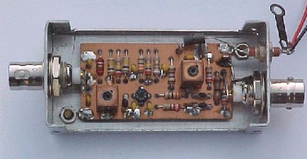
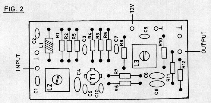
The amplifier is build on a double sided board measuring 25x50 mm. The upper side functions as a ground plane and the traces are on the lower side.The board can either be build into the radio or mounted in a small metal box with BNC connectors.
Electrical design
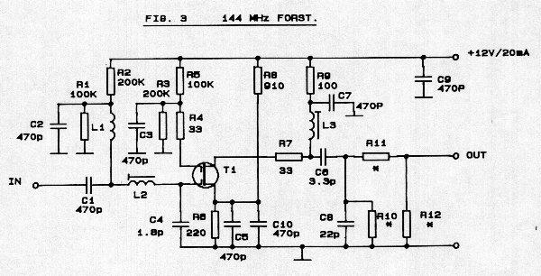
The diagram is shown below. The input circuit is a series transformation, the output circuit a "normal" parallel circuit with a capacitive output tap. As this amplifer has high gain, there is provision for a pi-attenuator on the output. Biasing of the transistor is done with a source resistor/voltage divider and with voltage dividers on both gate1 and gate2. This circuit tightly controls the DC parameters of the transistor.
Circuit details
The input circuit is a bit unusual as it uses a series inductor L2 to step the 50 ohm generator impedance up to 1600 ohm, which is the optimum gate impedance for noise matching. L2 resonates with C4 in parallel with the gate1 input capacitance.This minimises the loaded Q of the input circuit - important to keep insertion loss down - and the correct impedance (noise) match is fixed by design.
The output circuit is a parallel circuit with with L3, C6 and C8. The capacitive tap C6/C8 sets the drain impedance to 2 kohm. This also determines the gain.
Tune up
When powering up for the first time, start by checking the DC current consumption of abt. 20 mA. Then adjust L2 and L3 for maximum signal.For best noise match use a weak unmodulated signal and a receiver in FM mode. Then tune only L2 for best noise suppression.
By using a signal at the noise threshold, the FM (or PM) detector in the receiver will "amplify" any improvement of the C/N, so you can tune for optimum noisefigure by ear! Any resulting variation of the preamplifier gain will be nullified by the limiter in the FM receiver.
Attenuator
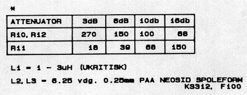
The can be taylored to your specific needs - which should be "not more than enough" - by having an attenuator at the output of the amplifier. The following table shows resistor values for different attenuation.
Performance
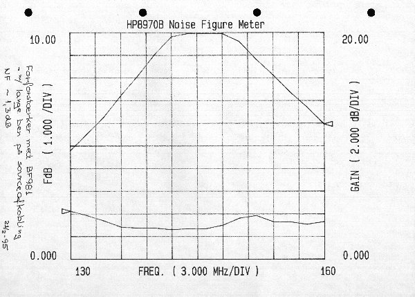
I have build and measured many of these amplifiers, and they have almost identical performance.The typical result with a 3-dB output attenuator is shown here:
PCB's and components
When I have the PCB layout converted to a proper file format, I'm going to post it here - until then the best I can offer, is a scan of the original artwork. Ask me.At the moment I'm unable to help with etched PCB's, however I still have the special Neosid coil forms and cans.
Back to OZ2OE homepage.